Overview
CB-CM5 is a 65 × 100 mm, four-layer carrier board for the Raspberry Pi Compute Module 5, drawn in KiCad 10. The CM5 brings the SoC, RAM and eMMC; the carrier's whole job is to take the two 100-pin board-to-board connectors the module lands on and turn them into connectors a human can plug into — without wrecking the signals on the way.
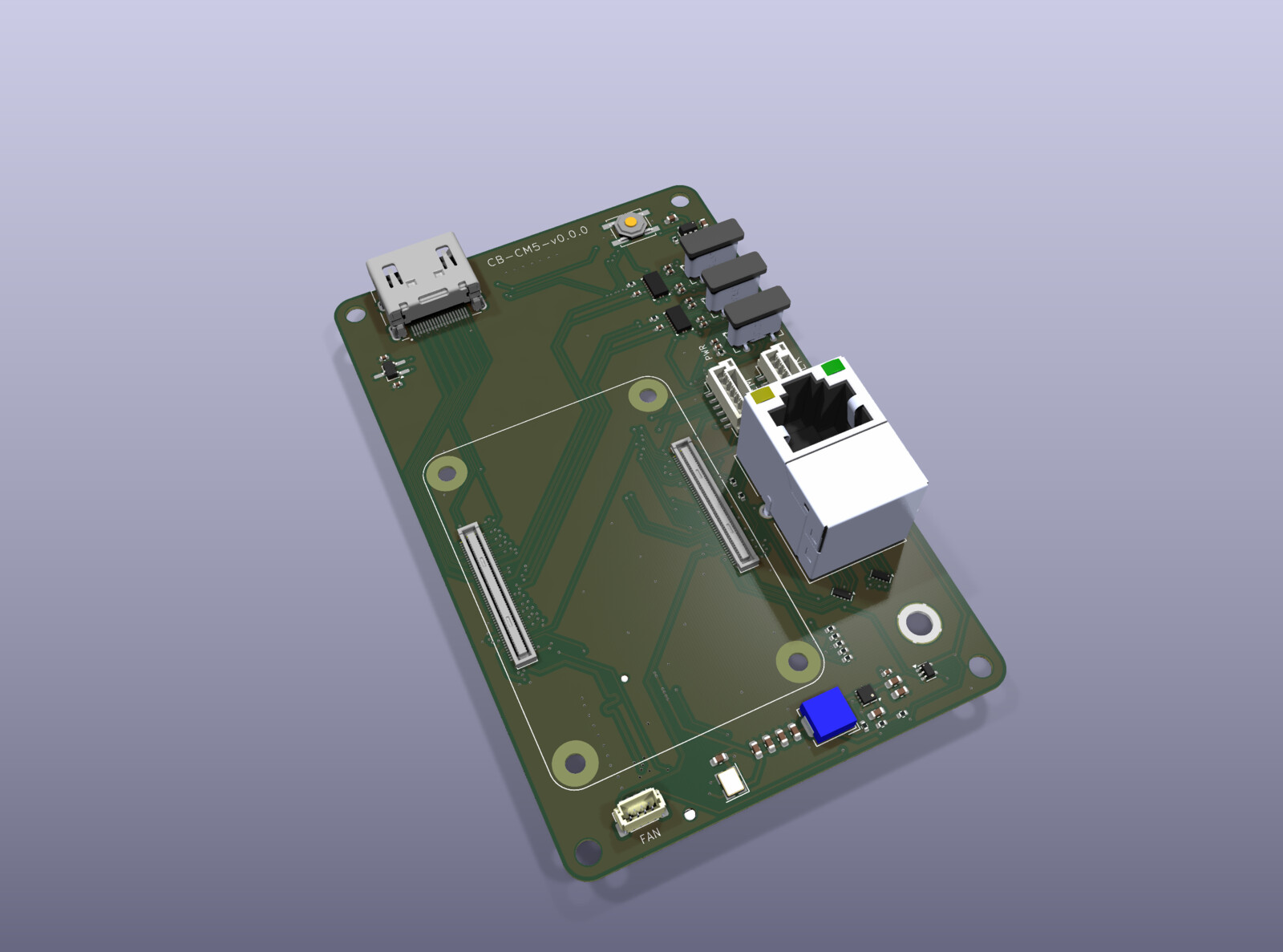
It was drawn for a drone. The idea was a Raspberry Pi doing real-time object detection in flight: a Hailo AI accelerator in the M.2 socket, a camera on one of the MIPI connectors, and the whole thing hanging off a flight computer for power and telemetry. That target chose most of the connectors on this board. It also explains the JST-GH headers, which latch — a requirement a desk never imposes and a drone imposes exactly once.
The drone was half the reason. The other half was that every fast bus on here — USB 3.0, gigabit Ethernet, HDMI, PCIe, MIPI D-PHY — was one I had never routed before. This is the first board where I had to think about impedance, stackups, differential pairs and length tuning at all, and putting five of those buses on one four-layer board was as much the point as the flying was.
The module mates through two Amphenol 10164227-1001A1RLF connectors, and the schematic is organized around that split, because the CM5 itself is:
- CM5A, pins 1–100 — Ethernet, GPIO, SD, UART, SPI, I²C, power control
- CM5B, pins 101–200 — PCIe, USB 3.0, HDMI, and the two MIPI D-PHY buses
Everything else on the board hangs off one of those two.
What comes out
| Ethernet | Gigabit, BEL V890-1AX1-A1 integrated magjack with link/activity LEDs |
| USB | 2 × USB-C 3.0 host ports (with orientation muxes), 1 × USB-C for USB 2.0 / OTG / power in |
| Display | 1 × HDMI Type-A, on a current-limited 5 V supply |
| Camera / display | 2 × 22-pin MIPI D-PHY FPC connectors (4 lanes + clock each) |
| Storage | M.2 M-key 2242 socket on a PCIe x1 link, plus microSD |
| Housekeeping | JST-GH power in, JST-GH telemetry UART, JST-SH 4-pin PWM fan, power button, status LEDs |
Note what is not here: no 40-pin GPIO header. The GPIO that leaves the board leaves through the two JST-GH connectors — a UART for telemetry and a power input — which is the tradeoff for keeping the board narrow and getting the connectors onto two edges instead of four. A drone has nothing to plug into a 40-pin header. It has a flight computer with a UART and a 5 V rail, and those are the two things it wants back.
It works
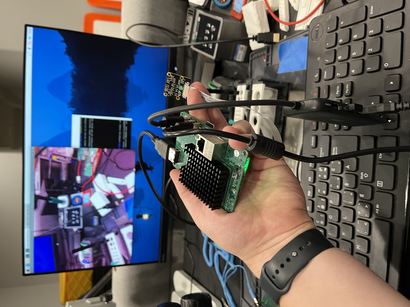
That's the board driving the monitor it's being photographed in front of, with a camera on one of the MIPI connectors, and USB enumerating at the same time. HDMI, D-PHY and USB all up at once, on a board whose silkscreen still reads CB-CM5-v0.0.0 — which turned out to be pessimistic.
The preview window is pointed at the bench. The first thing this board ever saw was the mess that produced it.
Design ran from late December 2024 through January 2025.
The schematic
All five sheets, parsed in your browser from the .kicad_sch sources on main. The folder icon in the left rail switches sheets; clicking a symbol opens its properties and footprint.
That isn't a screenshot of the schematic. It's the schematic — the same five files KiCad opens, fetched from the hardware repo and parsed client-side, so it can't drift out of date the way an exported PNG starts to the moment you export it.
Which also means the warts came along. Zoom in on the USB-C sheet and you'll find my own open questions still sitting there in blue text, unresolved. I left them in. A schematic with no notes on it is either finished or abandoned, and this one is neither.
Five sheets: a root that does almost nothing but wire the other four together, then one sheet per problem domain.
1 — Root
The top level is a patch panel. Four hierarchical sheets — usb_c, high_speed, low_speed, pcie_m2 — with the buses drawn between them so the interconnect is visible in one page: the two USB 3.0 groups going left to the port sheet, the PCIe group going right to the M.2 sheet, and the low-speed I²C/SPI/GPIO_VREF stubs dropping down.
The one real circuit here is a third USB-C receptacle. It carries only USB2_P/N and CC1/CC2 — no SuperSpeed pairs — so it lands directly on the CM5's own OTG port and CC pins. That makes it the port you flash the module through with rpiboot, and the port that feeds the +5 V rail. The JST-GH power header beside it offers the same 5 V for when a USB-C brick isn't what's powering the thing.
2 — High speed
The CM5B half of the module — pins 101 to 200, every differential pair on the board except Ethernet. Four things leave this sheet:
- HDMI → a Type-A 1.4 connector. Three data pairs, a clock pair, CEC, DDC, and hotplug detect. Its 5 V comes through an RT9742 current-limited load switch, so a display that inrushes hard browns out its own supply rather than the whole board. The CM5's second HDMI port is left unconnected.
- MIPI → two Hirose 22-pin FPC sockets carrying
DPHY0andDPHY1. Four data lanes and a clock lane each, plus a camera GPIO and an I²C bus per connector. These are the standard Pi camera/display pinout, so the same connector serves either direction. - PCIe → a single lane, its 100 MHz reference clock, and the four sideband signals (
nRST,nCLKREQ,nWAKE,PWR_EN) that go to the M.2 sheet. - USB 3.0 → two groups, each a SuperSpeed TX pair, an RX pair and a USB 2.0 pair, off to the port sheet.
GPIO_VREF is set here by a divider off the DDC lines, and a 2.2k resistor pulls the second camera's I²C up to 3.3 V.
3 — Low speed
The busiest sheet, and the one that decides what the board actually is. "Low speed" is doing a lot of work as a label — it's the sheet where gigabit Ethernet lives, which is only slow relative to its neighbours.
- Gigabit Ethernet — the four
TRDpairs run from the CM5 through a pair of TPD4EUSB30 ESD arrays into a BEL V890-1AX1-A1 integrated magjack. Link and activity LEDs are driven from the module's ownEthernet_nLEDoutputs through 470 Ω. - microSD — a Hirose push-push socket with card detect. Its 3.3 V comes through a second RT9742 switch, gated by the CM5's
SD_PWR_ON, so the card can be power-cycled in software. A note on the sheet records the constraint that matters: SD signals are only available on modules without eMMC. - Boot and config straps — five 0 Ω links set
USBOTG_ID,PMIC_ENABLE,SYNC_OUT,EEPROM_nWPandnRPIBOOT. A sixth pair of 0 Ω links — one fitted, one marked do-not-populate — selects whetherGPIO_VREFsits at 3.3 V or 1.8 V. That's a link option, not a runtime one, and one you get exactly one chance to solder correctly. - Housekeeping — a power button, an activity LED, a power LED buffered through a 74LVC1G07 open-drain gate, and a 4-pin JST-SH fan header with PWM out and tacho back in.
- GPIO — most of the 28 GPIOs are deliberately left unconnected. The ones that escape are UART2 (
TELEM_TX/RX/CTS/RTS) to the JST-GH telemetry connector, SPI0, and I²C.
4 — PCIe / M.2
An M.2 M-key socket sized for 2242 modules — the form factor both an NVMe drive and the Hailo accelerator arrive in — wired for one lane: PETn0/p0 and PERn0/p0 connected, lanes 1 through 3 explicitly unconnected, because one lane is all the CM5 exposes. The other three pin groups on that connector are there to remind you what you're not getting.
The interesting half of this sheet is the power. NVMe drives can pull well over an amp in burst, which is more than you want to take off a shared 3.3 V rail, so the socket gets its own — an AP3441 synchronous buck stepping 5 V down through a 2.2 µH inductor to a dedicated M2_3v3, with a 10k/2.2k feedback divider, 4×10 µF of output bulk, and an enable tied to the CM5's PCIE_PWR_EN. The drive powers up when the host says so, and its current never crosses the rest of the board.
An Abracon 32.768 kHz oscillator feeds SUSCLK, which is what lets an NVMe drive run its low-power suspend states instead of just being on or off.
5 — USB-C
Two identical channels, one per USB 3.0 port. The problem each solves is that USB-C is reversible and USB 3.0 is not — the SuperSpeed pairs land on different pins depending on which way the plug went in.
- The muxes — an HD3SS3212 SuperSpeed 2 mux per port — physically swap the TX and RX pairs to match the plug orientation, with 100 nF AC-coupling caps on the SuperSpeed lines.
- The CC controllers — a TUSB322I per port — are what tell the mux which way that was. They read the CC pins, decide the port is a downstream-facing host, and drive the mux's
SEL. - One AP2553 current-limited switch, with a 15k ILIM resistor, supplies VBUS to both ports from the 5 V rail. Same reasoning as the HDMI switch: a peripheral that draws too much trips the switch instead of dragging the CM5's supply down with it.
The mux is a quiet admission that I would rather let a two-dollar part decide the orientation than argue about it in the layout. It also turns TX/RX from a fixed assignment into a routing convenience, which is the other note in blue on that sheet — a reminder to go back and confirm which way round I'd actually drawn it.
Stackup and routing
The board file itself — 2.1 MB of .kicad_pcb, parsed in the browser. The layers icon in the left rail toggles F.Cu, In1.Cu, In2.Cu and B.Cu independently; every claim in this section is checkable in there.
The feature list is the excuse. On a CM5 carrier the hard part is entirely in the physical layer — once PCIe, two USB 3.0 groups, HDMI and two MIPI buses are leaving the same connector, the schematic is the easy half and the board is where it gets decided. None of which I had done before, which is why the board was worth drawing at all.
Turn off everything but F.Cu in the frame above and the shape of the problem shows up immediately: the diagonal fanout leaving both CM5 connectors is most of the high-speed routing on the board, and it all had to happen in the couple of millimetres between two 100-pin connectors before anything could head for an edge.
The stackup
Four layers on 0.8 mm total thickness instead of the usual 1.6 mm, and the dielectric numbers are the design, not a default. They come from choosing one of JLCPCB's impedance-controlled stackups — the 3313-prepreg one — before routing anything, because the ordinary stackup doesn't guarantee what sits between the layers. Without a known prepreg thickness and a known εr, every trace width you calculate is a guess with a decimal point on it.
| Layer | Thickness | εr | |
|---|---|---|---|
| F.Cu | signal + GND pour | 35 µm | |
| prepreg | 99.4 µm | 4.1 | |
| In1.Cu | GND plane | 15.2 µm | |
| core | 450 µm | 4.6 | |
| In2.Cu | GND plane | 15.2 µm | |
| prepreg | 99.4 µm | 4.1 | |
| B.Cu | signal + GND pour | 35 µm |
The 0.8 mm is for the drone. The number that matters electrically is the 99.4 µm of 3313 prepreg between each signal layer and the plane under it: pushing the reference that close is what lets a 100 Ω differential pair be ~0.1 mm wide instead of ~0.25 mm, and on a board this dense that's the difference between the fanout fitting and not fitting. The 450 µm core in the middle only sets how far apart the two ground planes sit, which nothing on here cares about.
One geometry per bus
Every high-speed bus has its own netclass, because every one of them targets a different impedance:
| Netclass | Track | Pair width | Pair gap |
|---|---|---|---|
pcie | 0.135 mm | 0.134 mm | 0.100 mm |
usb | 0.114 mm | 0.114 mm | 0.100 mm |
hdmi | 0.106 mm | 0.100 mm | 0.150 mm |
csi | 0.200 mm | 0.100 mm | 0.215 mm |
low_speed | 0.200 mm | 0.200 mm | 0.250 mm |
Those aren't round numbers, which is the point — they're solved from the stackup above for the impedance each standard asks for: 85 Ω for PCIe, 90 Ω for USB, 100 Ω for HDMI and MIPI. The MIPI pairs are the loosely-coupled ones, wide gap and narrow trace, because D-PHY cares more about the single-ended impedance of each lane than about coupling between them.
Getting this wrong doesn't fail loudly. It reflects, and the reflections show up as a link that trains at a lower speed, or works on three boards out of five — a failure mode with no error message, no log line, and no way to bisect it.
Length matching
Impedance gets a pair to the far end intact. Length matching is what makes both halves of it arrive at the same time.
Inside a pair the tolerance is tight, and the fanout is where it gets lost: the two sides of a pair leave the connector on pins that aren't equidistant from wherever they're headed, so one leg always comes out short. Skew within a pair doesn't just delay the edge — it turns differential signal into common-mode, which is the mode a receiver can't reject and the mode that leaves the board as radiation.
Between pairs, how much you care depends entirely on the bus:
- PCIe and USB 3.0 — nearly nothing to do. One PCIe lane, and each USB port is independent, so there's no sibling lane to line up against. The clock is recovered from the data.
- HDMI — three data pairs against a forwarded clock pair, so all four have to agree with each other.
- MIPI D-PHY — the same shape: four data lanes referenced to a clock lane travelling alongside them.
Which is a convenient accident on this board. The two fastest buses on it are the two with the loosest inter-pair requirements, and the two that genuinely need matching both run to connectors on a board edge, where there is room to put the tuning.
You can count where that room got spent — there are thirteen tuning patterns on the board, and they land about where the argument above predicts:
| Where | Count | Doing what |
|---|---|---|
| Around the HDMI connector | 3 | four pairs agreeing with each other |
| Under the first camera FPC socket | 5 | four D-PHY lanes against their clock |
| Above the M.2 socket | 4 | PCIe, intra-pair only |
| By the USB muxes on the right edge | 1 | one pair, one leg short out of the fanout |
The PCIe entries aren't a contradiction of what I just said. Inter-pair matching is what a single lane doesn't need; the two halves of that lane still have to arrive together, and the fanout still robs one of them. Intra-pair tuning is the tax every differential pair pays, forever, regardless of how relaxed its bus is about its neighbours.
Signals outside, ground inside
The routing is deliberately lopsided:
| Layer | Track segments | Contents |
|---|---|---|
| F.Cu | 1435 | signals, GND pour |
| In1.Cu | 57 | GND plane, +5 V and +3.3 V distribution |
| In2.Cu | 0 | GND plane, untouched |
| B.Cu | 877 | signals, GND pour |
Every signal lives on an outer layer, referenced to the plane 99.4 µm beneath it. Current goes out on a trace and comes back on that plane directly underneath; split the plane, or route a pair across a gap in it, and the return current has to detour around — which is a loop, and a loop is an antenna.
That table is the whole argument, and it's the one thing the layer toggles show better than any picture. Isolate In1.Cu and you'll see the 57 segments: +5 V and +3.3 V distribution, each one a slot in the plane, all of them confined to the top-right corner and the right edge where the USB-C power switching lives. The diagonal fanout region under the CM5 connectors — where the PCIe, HDMI and MIPI pairs all are — sits over intact copper. Isolate In2.Cu and there is nothing on it at all, which is the point: anything routed on the bottom gets a genuinely unbroken reference.
Rules
Fabrication limits were set to a 4-layer prototype process and then actually used: 90 µm minimum trace and clearance, 0.45/0.30 mm vias, 75 µm minimum annular ring, 0.5 mm copper-to-edge. 322 vias in total.
None of this shows up in a photo of the finished board, which is exactly why it was the project. There's no partial credit and no way to fix it in firmware later, and the frame at the top of this section is the only honest way to show any of it.
Which leaves the part a photo is good for.
The board
92 footprints, 65 on the top and 27 on the bottom. The split isn't arbitrary — everything a cable plugs into lives on top, and everything that either lies flat or wants to be out of the way lives underneath. Placement came first and the routing above had to live with it, which is the usual order and the usual regret.
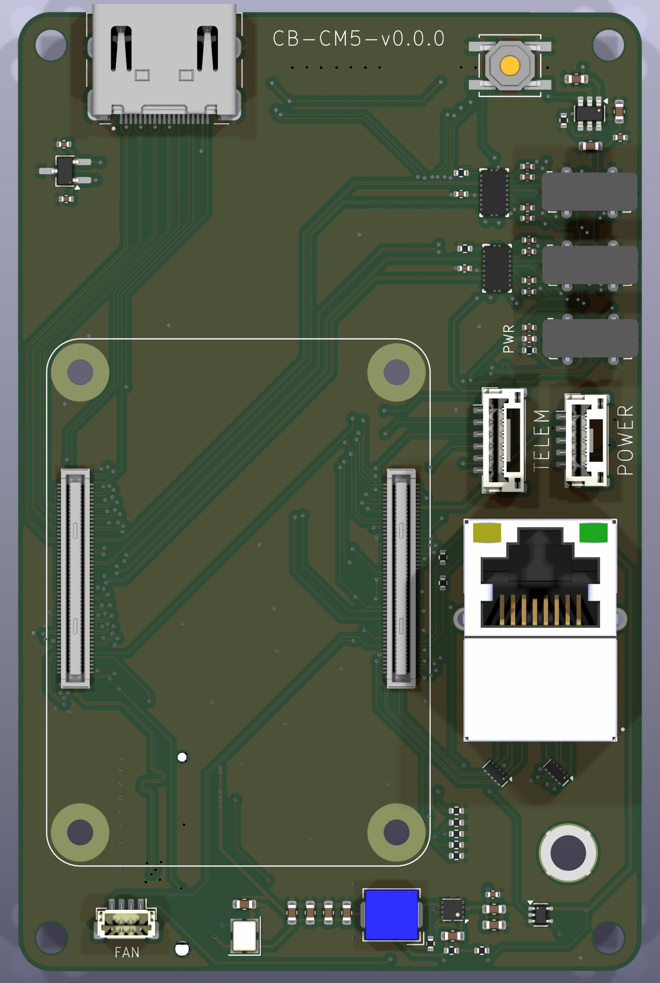
The two 100-pin CM5 connectors run vertically through the center, and the white silkscreen rectangle around them is the module's own outline — the CM5 sits over most of the board, which is why the right-hand third is where all the connectors ended up. The four M3 holes at the corners are the mounting pattern; the four plated pads inside the outline are the module's.
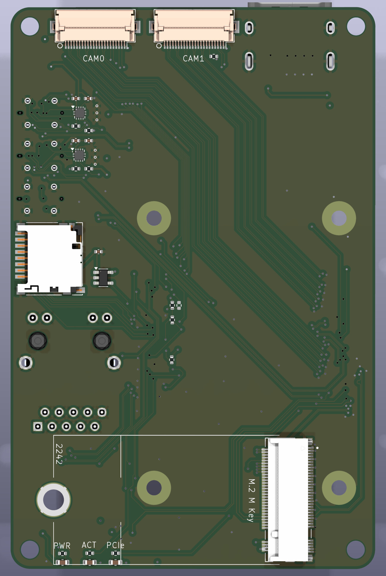
Underneath: the two 22-pin camera FPC sockets (CAM0, CAM1) at the back edge where a ribbon can fold flat, the microSD socket, the M.2 2242 socket with its keep-out and standoff silkscreened in, and the small parts that support the top-side connectors — the two TUSB322I CC controllers, the SD card's load switch, and the three status LEDs.
Putting the M.2 socket on the bottom is what makes a 65 mm-wide board possible. A 2242 drive is 42 mm long, and there is nowhere on the top surface it could go without either colliding with the CM5 or pushing the board out past 80 mm. Layout is mostly this: an argument with a rectangle you agreed to before you knew what was going in it.